
CVD Diamond for High-Performance Thermal Management
CVD diamond thermal management solutions help improve heat spreading and thermal control for demanding GaN, RF, laser, power electronics, and semiconductor applications. Single crystal and polycrystalline CVD diamond materials are available for projects requiring high thermal conductivity, electrical insulation, precision surfaces, and application-specific geometry.
Move Heat Away from the Device More Efficiently
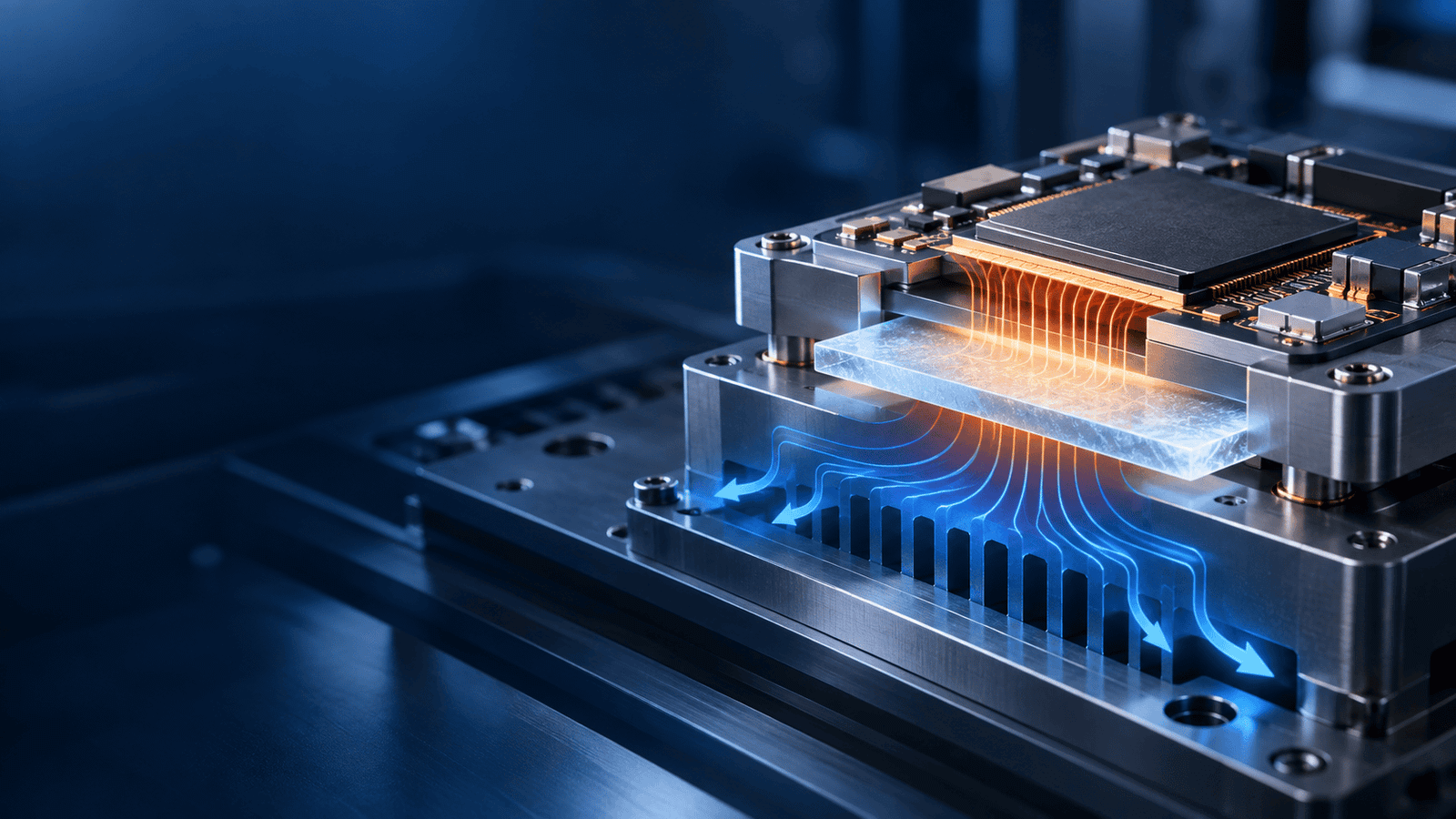
CVD diamond can be positioned within the thermal path between a high-power device and the downstream cooling structure. Material type, dimensions, thickness, surface quality and interface design should be reviewed together.
Heat Source
Identify the device, heat-generating area and operating conditions.
Diamond Layer
Select single crystal or polycrystalline CVD diamond based on thermal performance and available size.
Thermal Interface
Review flatness, surface roughness, metallization and bonding requirements.
Heat Rejection
Integrate the diamond component with the downstream thermal structure.
Three Ways to Start a Thermal Project
CVD Diamond Heat Spreaders
Heat spreader projects can use either single crystal or polycrystalline CVD diamond, depending on performance, size and integration needs.
Single Crystal CVD Diamond
Higher thermal performance, higher electrical resistivity and precision surface capability.
Polycrystalline CVD Diamond
Larger available size combined with high thermal performance and strong cost-performance.
Thermal Material Reference
Core reference values used throughout JingChuang CVD thermal-management pages.
| Parameter | Polycrystalline CVD Diamond | Single Crystal CVD Diamond |
|---|---|---|
| Thermal Conductivity | ≥1000 / ≥1500 / >1800 W/(m·K) @ 293 K |
≥1600 / ≥1800 /
≥2000 / ≥2200 W/(m·K) @ 293 K
High-end reference: 2400–2600 W/(m·K) |
| Thermal Diffusivity | >5.5 / ≥8.3 / ≥10.0 cm²/s @ 300 K | ≥10.0 / ≥11.0 / ≥12.0 cm²/s @ 300 K |
| Thermal Expansion | 1.0 ± 0.1 ppm/K @ 300 K | 1.0 ± 0.1 ppm/K @ 300 K |
| Volume Resistivity | ≥1×10¹² Ω·cm | ≥1×10¹³ Ω·cm |
| Thickness | 0.10–1.00 mm | 0.05–5.50 mm |
| Available Size | Large-size mass production; up to 8 inches | Mainstream 10×10 mm; high-end customization up to 20×20 mm |
| Polished Surface Roughness | Ra ≤20 / 50 nm |
Ra ≤5 / 10 / 20 nm
Ultra-precision: 0.5–1 nm |
| Flatness | ≤1 μm over 10 mm |
≤1 μm over 10 mm
Precision reference: 0.5 μm / 10 mm |
Thermal Management Across High-Performance Systems
CVD diamond material selection depends on thermal load, available size, interface conditions, surface requirements and system integration.
GaN / RF
CVD diamond materials can be reviewed for high-frequency thermal-management projects.
High-Power Laser
Single crystal diamond is a natural starting point where higher thermal performance and surface precision matter.
Power Electronics
Diamond thermal materials can be reviewed around device geometry, insulation and thermal-transfer requirements.
Semiconductor Thermal Management
Single crystal and polycrystalline options can be selected according to required size and thermal performance.
From Heat Source to Diamond Material Specification
Define the Application
Identify the device, thermal source and operating environment.
Select Material Route
Compare single crystal, polycrystalline or a finished heat spreader configuration.
Define Geometry
Confirm size, thickness, tolerance, flatness and surface finish.
Confirm Integration
Review metallization, bonding and quality documentation.
Surface, Flatness & Metallization Matter
Surface Finish
Single crystal and polycrystalline materials have different polished and lapped surface capabilities.
Flatness & Thickness
Thickness and flatness should be selected around the actual interface and geometry requirement.
Metallization
Reference options include Ti/Pt/Au, Ti/Au, W and Mo, with TiW/Au also listed for single crystal material.
What to Send for a Thermal Management Review
Send the complete system requirement rather than only asking for the highest thermal conductivity grade.
Thermal Project Review
Submit Requirements
Application, dimensions, thermal requirement and drawing.
Material Review
Compare single crystal, polycrystalline and heat spreader routes.
Specification Review
Confirm size, thickness, surface and integration requirements.
Quotation
Quotation follows the confirmed technical specification.
Material Documentation & Testing Support
CoA & Documentation
CoA documentation is available for CVD diamond materials.
- Certificate of Analysis
- Project-specific documentation
- Inspection requirements reviewed during technical review
Testing Support
Testing can be aligned with confirmed project requirements.
- Raman spectroscopy
- Thermal performance
- Flatness
- Surface roughness
- Electrical resistivity
Explore CVD Diamond Thermal Materials
CVD Diamond Thermal Management Questions
What thermal conductivity grades are available?
Polycrystalline reference grades are ≥1000, ≥1500 and >1800 W/(m·K) at 293 K. Single crystal reference grades are ≥1600, ≥1800, ≥2000 and ≥2200 W/(m·K), with high-end reference values of 2400–2600 W/(m·K).
Which material should I use for the highest thermal performance?
Single crystal CVD diamond provides the higher reference thermal-performance range. Final selection should still consider available size, thickness, surface and integration requirements.
Which material is better for larger components?
Polycrystalline CVD diamond has the larger available-size advantage, with the reference specification supporting sizes up to 8 inches.
Can the material be metallized?
Yes. Reference options include Ti/Pt/Au, Ti/Au, W and Mo. TiW/Au is also listed for single crystal material.
Can I submit a complete thermal drawing for review?
Yes. Submit your application, dimensions, thickness, thermal requirement, surface condition, quantity and drawing through the RFQ form.
Is testing documentation available?
CoA documentation is available and testing can be supported according to confirmed project requirements.
Have a Thermal Management Requirement?
Send your application, dimensions, thickness, thermal target, surface requirement and drawing. JingChuang CVD can review the appropriate material route before quotation.