
Polycrystalline CVD Diamond for Large-Area Thermal Management
Free-standing polycrystalline CVD diamond produced by MPCVD, combining high thermal conductivity, large-area availability and flexible project-specific processing options.
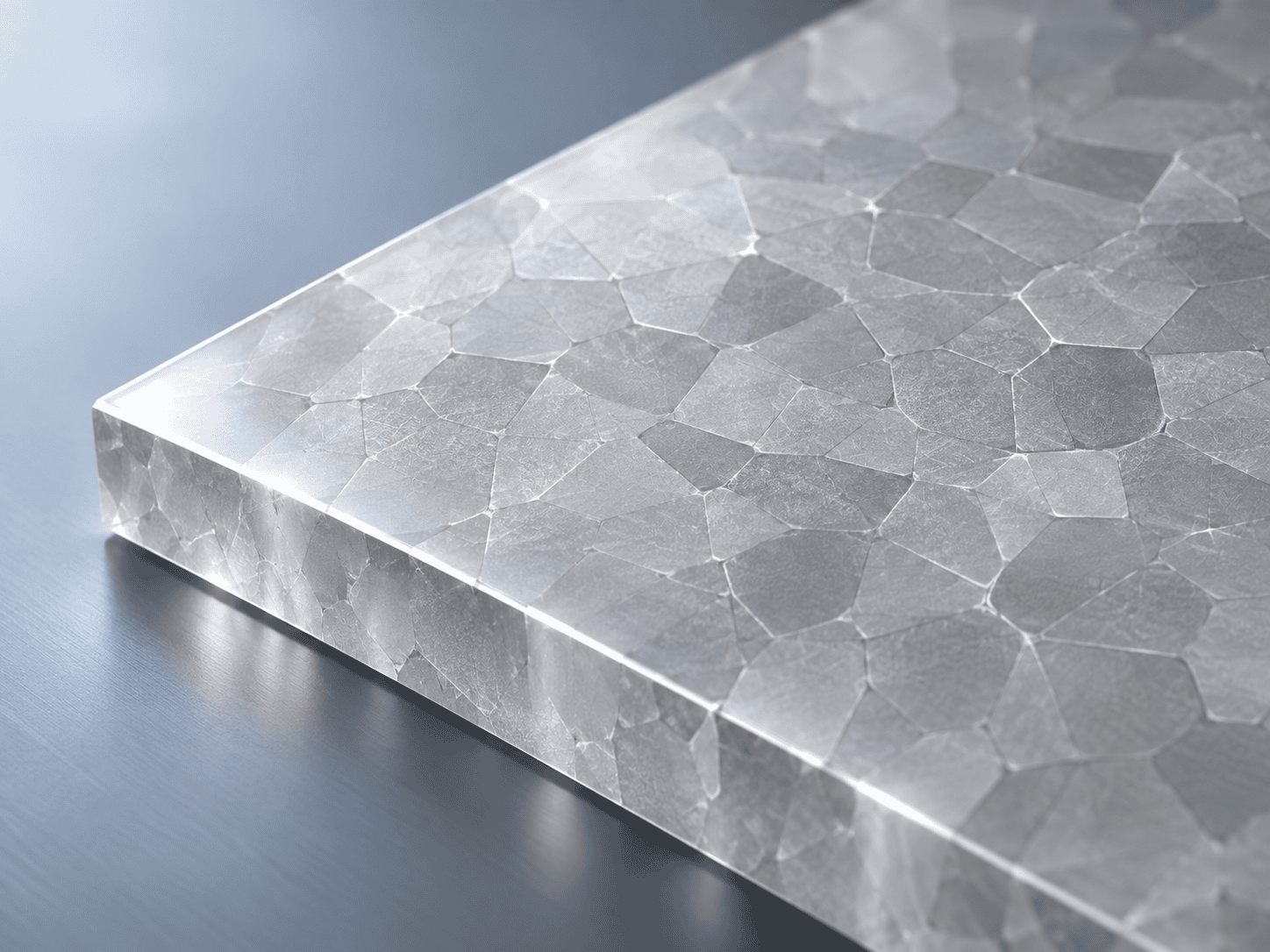
Free-Standing Polycrystalline CVD Diamond
Polycrystalline CVD diamond provides high thermal conductivity while supporting larger available sizes than single crystal material, making it suitable where larger-area diamond components are required.
MPCVD Growth
Microwave plasma chemical vapor deposition for free-standing polycrystalline material.
Large-Area Availability
Supports large-size mass production, with reference maximum size up to 8 inches.
Thermal Performance
Multiple thermal conductivity grades are available for project selection.
Cost-Performance Balance
Polycrystalline material offers an advantage for larger-size applications where overall cost-performance matters.
Core Polycrystalline Material Parameters
Reference values under standard room-temperature conditions. Final requirements should be confirmed during project technical review.
Reference grades: ≥1000 / ≥1500 / >1800
Polycrystalline CVD Diamond Technical Reference
The following values are reference parameters for standard mass-production material.
| Parameter | Polycrystalline CVD Diamond | Project Notes |
|---|---|---|
| Material Type | Free-standing Polycrystalline CVD Diamond | Material grade selected according to project requirements. |
| Growth Method | MPCVD — Microwave Plasma Chemical Vapor Deposition | Standard growth method. |
| Thermal Conductivity | ≥1000 / ≥1500 / >1800 W/(m·K) @ 293 K | Grade-dependent. |
| Thermal Diffusivity | >5.5 / ≥8.3 / ≥10.0 cm²/s @ 300 K | Grade-dependent. |
| Coefficient of Thermal Expansion | 1.0 ± 0.1 ppm/K @ 300 K | Standard room-temperature reference. |
| Volume Resistivity | ≥1×10¹² Ω·cm | Standard reference value. |
| Thickness Range | 0.10–1.00 mm | Custom thickness review available. |
| Thickness Tolerance | ±0.025 mm / ±0.05 mm | Final tolerance according to project requirements. |
| Maximum Available Size | Large-size mass production; reference maximum up to 8 inches | Final available geometry subject to technical review. |
| Polished Surface Roughness | Ra ≤20 / 50 nm | Surface requirement should be specified with RFQ. |
| Lapped Surface Roughness | Ra ≤200 / 250 nm | Lapped surface reference. |
| Flatness | ≤1 μm over 10 mm | Standard precision reference. |
| Dimensional Tolerance | ±0.05 mm or +0.20 / -0 mm | Drawing-dependent. |
| Metallization | Ti/Pt/Au, Ti/Au, W, Mo | Available according to project requirements. |
| Quality Documentation | CoA available; third-party testing available | Documentation requirements can be confirmed during review. |
Why Polycrystalline CVD Diamond?
Large Available Size
Polycrystalline CVD diamond supports significantly larger available dimensions than single crystal material.
High Thermal Conductivity
Multiple thermal conductivity grades support different thermal-performance requirements.
Surface Processing Options
Polished and lapped surface conditions can be selected according to project needs.
Cost-Performance Advantage
Polycrystalline material is advantageous where larger dimensions and overall cost-performance are important.
When Polycrystalline CVD Diamond Fits the Project
Polycrystalline material is generally preferred where larger available size and cost-performance are important selection factors.
Larger Components
Suitable where the required dimensions exceed practical single crystal sizes.
Thermal Management
High thermal conductivity grades can support thermal-spreading projects.
Cost-Performance Projects
Useful where thermal performance and larger material size must be balanced with overall project economics.
Custom Dimensions
Submit target geometry, thickness and drawing for project-specific review.
Submit Your Requirements for Technical Review
Provide the full project requirement so material grade, dimensions, thickness, surface condition and optional metallization can be reviewed together.
Project Review Process
Submit Requirements
Application, dimensions, thickness, quantity and drawing.
Technical Review
Review thermal grade, size, surface and processing requirements.
Specification Confirmation
Confirm feasible material and product specifications.
Quotation
Quotation follows the confirmed technical requirements.
Documentation & Testing Support
CoA Documentation
Certificate of Analysis documentation is available according to product and project requirements.
- CoA available
- Project-specific documentation
- Inspection requirements reviewed before quotation
Third-Party Testing
Third-party testing is available according to project requirements.
- Testing requirements can be defined during review
- Documentation aligned with confirmed project needs
- Final scope confirmed before production
Compare CVD Diamond Materials
Polycrystalline CVD Diamond Questions
What thermal conductivity grades are available?
Reference grades are ≥1000, ≥1500 and >1800 W/(m·K) at 293 K. Final grade should be confirmed during technical review.
What thickness range is available?
The reference thickness range is 0.10–1.00 mm, with customization reviewed according to project requirements.
How large can polycrystalline CVD diamond be?
The specification reference states that large-size mass production is supported, with maximum available size up to 8 inches. Final geometry should be technically reviewed.
What surface roughness is available?
Reference polished surface roughness is Ra ≤20 / 50 nm. Lapped surface roughness is Ra ≤200 / 250 nm.
Is metallization available?
Reference metallization options include Ti/Pt/Au, Ti/Au, W and Mo. Final structure should be confirmed according to project requirements.
Is quality documentation available?
CoA documentation and third-party testing are available according to project requirements.
Need a Polycrystalline CVD Diamond Material Review?
Send your target dimensions, thickness, thermal requirement, surface condition, quantity and drawing for technical review.