
Single Crystal vs Polycrystalline CVD Diamond
Compare thermal performance, electrical resistivity, available size, thickness, surface finish, flatness and metallization to select the appropriate CVD diamond material for your project.
Which CVD Diamond Material Should You Start With?
Choose Single Crystal
Start with single crystal CVD diamond when the project prioritizes higher thermal conductivity, higher electrical resistivity or ultra-precision surface quality.
- High-end chips
- Laser devices
- High-frequency equipment
- Precision bonding
- High-insulation requirements
Choose Polycrystalline
Start with polycrystalline CVD diamond when larger available dimensions and overall cost-performance are important.
- Larger-area diamond components
- Large-area heat spreading
- Projects requiring larger available size
- Cost-performance driven applications
- Custom large-area geometry
Two CVD Diamond Material Routes
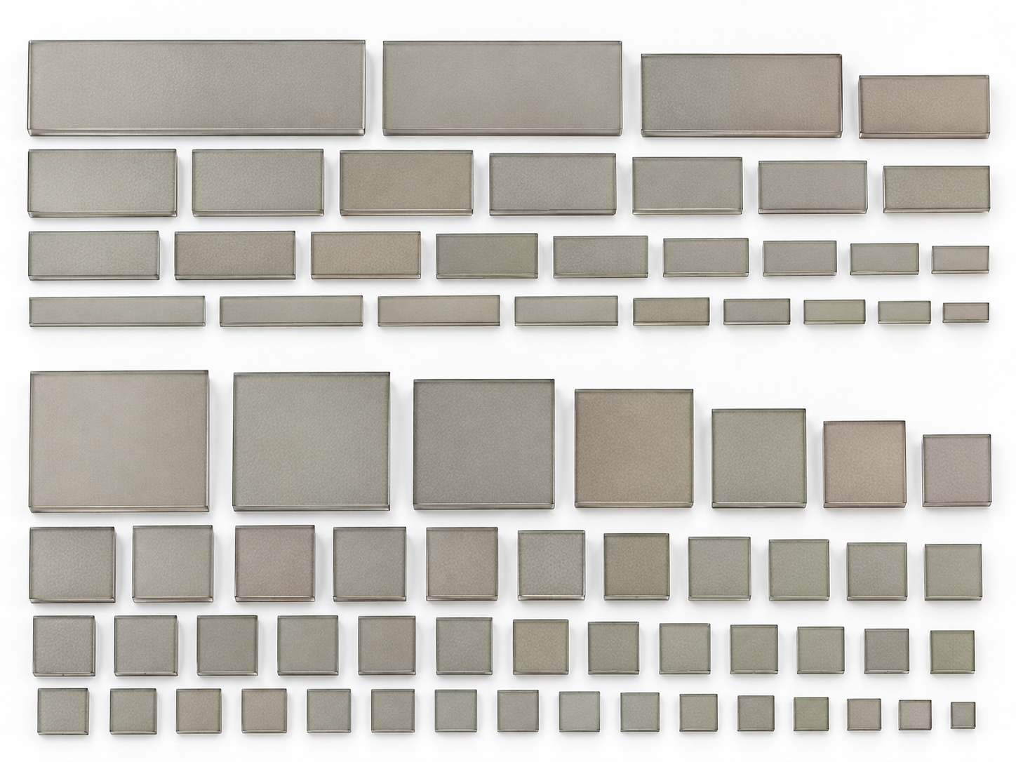
Single Crystal CVD Diamond
Free-standing single crystal CVD diamond produced by MPCVD. Its complete crystal lattice and absence of grain boundaries support higher thermal performance, higher electrical resistivity and precision polishing.
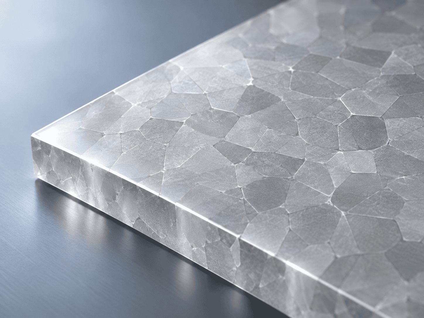
Polycrystalline CVD Diamond
Free-standing polycrystalline CVD diamond produced by MPCVD. Its main advantage is larger available size combined with strong thermal performance and cost-performance.
Single Crystal vs Polycrystalline CVD Diamond
Reference technical parameters for standard room-temperature conditions.
| Parameter | Polycrystalline CVD Diamond | Single Crystal CVD Diamond |
|---|---|---|
| Material Type | Free-standing Polycrystalline CVD Diamond | Free-standing Single Crystal CVD Diamond |
| Growth Method | MPCVD | MPCVD |
| Thermal Conductivity | ≥1000 / ≥1500 / >1800 W/(m·K) @ 293 K |
≥1600 / ≥1800 / ≥2000 / ≥2200
W/(m·K) @ 293 K
High-end reference: 2400–2600 W/(m·K) |
| Thermal Diffusivity | >5.5 / ≥8.3 / ≥10.0 cm²/s @ 300 K | ≥10.0 / ≥11.0 / ≥12.0 cm²/s @ 300 K |
| Coefficient of Thermal Expansion | 1.0 ± 0.1 ppm/K @ 300 K | 1.0 ± 0.1 ppm/K @ 300 K |
| Volume Resistivity | ≥1×10¹² Ω·cm |
≥1×10¹³ Ω·cm
Intrinsic undoped reference |
| Thickness Range | 0.10–1.00 mm | 0.05–5.50 mm |
| Thickness Tolerance | ±0.025 mm / ±0.05 mm |
±0.025 mm / ±0.05 mm
Precision parts: ±0.015 mm |
| Maximum Available Size | Supports large-size mass production; up to 8 inches | Mainstream 10×10 mm; high-end customization up to 20×20 mm |
| Polished Surface Roughness | Ra ≤20 / 50 nm |
Ra ≤5 / 10 / 20 nm
Ultra-precision reference: 0.5–1 nm |
| Lapped Surface Roughness | Ra ≤200 / 250 nm | Ra ≤200 nm |
| Flatness | ≤1 μm over 10 mm |
≤1 μm over 10 mm
Precision polished reference: 0.5 μm / 10 mm |
| Dimensional Tolerance | ±0.05 mm or +0.20 / -0 mm | ±0.05 mm or +0.20 / -0 mm |
| Metallization | Ti/Pt/Au, Ti/Au, W, Mo | Ti/Pt/Au, Ti/Au, TiW/Au, W, Mo |
| Quality Documentation | CoA available; third-party testing available | CoA available; third-party testing supported |
The Four Differences That Matter Most
Thermal Performance
Single crystal CVD diamond has a complete crystal lattice without grain boundaries, supporting higher thermal performance than polycrystalline material.
Electrical Insulation
Single crystal material has a higher reference volume resistivity, making it suitable for projects with higher insulation requirements.
Surface Precision
Single crystal material supports lower surface roughness and ultra-precision polishing for optical and precision bonding applications.
Available Size
Polycrystalline CVD diamond supports significantly larger available sizes, giving it an advantage in larger-area applications.
Select by Project Requirement
Do not select CVD diamond by one number alone. Review thermal requirement, size, surface and integration requirements together.
Thermal Requirement
Define the target thermal performance or device-level thermal requirement.
Required Size
Determine whether the project can use single crystal dimensions or needs larger-area material.
Surface Precision
Define polished or lapped surface, roughness and flatness requirements.
Integration
Confirm dimensions, tolerance, metallization and quality documentation.
Material Selection by Application
High-End Chips
Single crystal material is preferred where higher thermal performance is the main requirement.
Laser Devices
Higher thermal performance and precision surface quality make single crystal suitable for demanding laser applications.
High-Frequency Equipment
Higher thermal conductivity and electrical resistivity support high-performance electronic environments.
Larger-Area Components
Polycrystalline material is the natural starting point when the required dimensions exceed single crystal sizes.
Large-Area Heat Spreading
Larger available size combined with high thermal conductivity supports larger-area thermal projects.
Custom Applications
Where thermal performance, size, surface condition and cost must all be balanced, submit the complete specification for technical review.
What to Send Before Material Selection
Providing the complete project requirement helps avoid selecting material based only on thermal conductivity.
Material Review Process
Submit Project Requirements
Application, drawing, dimensions and technical requirements.
Compare Material Routes
Review single crystal versus polycrystalline suitability.
Confirm Specifications
Confirm material grade, geometry, surface and documentation.
Quotation
Commercial quotation follows the confirmed specification.
Documentation & Testing Support
CoA
Certificate of Analysis documentation is available for CVD diamond material.
Third-Party Testing
Third-party testing can be supported according to project requirements.
Inspection Items
For single crystal material, documentation can include Raman, thermal performance, flatness, roughness and resistivity testing.
Continue to the Product Pages
CVD Diamond Material Selection Questions
Which material has higher thermal conductivity?
Single crystal CVD diamond has higher reference thermal performance. The listed single crystal grades are ≥1600, ≥1800, ≥2000 and ≥2200 W/(m·K) at 293 K, with high-end reference values of 2400–2600 W/(m·K).
Which material is better for larger sizes?
Polycrystalline CVD diamond has a clear size advantage. The reference specification supports large-size mass production up to 8 inches.
Which material has better surface finish?
Single crystal CVD diamond supports lower polished surface roughness. Its reference polished values are Ra ≤5 / 10 / 20 nm, with ultra-precision reference values of 0.5–1 nm.
Which material has higher electrical resistivity?
The reference value for polycrystalline CVD diamond is ≥1×10¹² Ω·cm, while intrinsic undoped single crystal material is ≥1×10¹³ Ω·cm.
Can both materials be metallized?
Yes. Polycrystalline reference options include Ti/Pt/Au, Ti/Au, W and Mo. Single crystal options also include TiW/Au.
Can I send a drawing instead of choosing a material myself?
Yes. Send your application, dimensions, thickness, thermal requirement, surface requirement and drawing. Material selection can then be reviewed before quotation.
Not Sure Which CVD Diamond Material to Choose?
Send your application, drawing, dimensions, thermal target and surface requirements. JingChuang CVD can review the material route before quotation.