
Single Crystal CVD Diamond for High-Performance Thermal & Precision Applications
Free-standing single crystal CVD diamond produced by MPCVD, supporting high thermal conductivity, high electrical resistivity, precision surface finishing and application-specific dimensions.
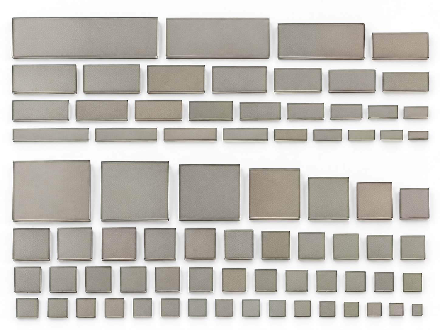
Free-Standing Single Crystal CVD Diamond
Single crystal CVD diamond combines a continuous crystal lattice without grain boundaries with high thermal conductivity, high electrical resistivity and the ability to achieve precision polished surfaces.
MPCVD Growth
Microwave plasma chemical vapor deposition for free-standing single crystal material.
High Thermal Performance
Multiple thermal conductivity grades are available for thermal-management projects.
Precision Surface Finish
Polished, lapped and ultra-precision finishing options according to project need.
Custom Geometry
Thickness, dimensions and project geometry reviewed according to drawings and use case.
Core Single Crystal Material Parameters
Reference values under standard room-temperature conditions. Project-specific requirements should be submitted for technical review.
High-end reference: 2400–2600 W/(m·K)
Single Crystal CVD Diamond Technical Reference
The following values are reference parameters for standard mass-production material and precision options.
| Parameter | Single Crystal CVD Diamond | Project Notes |
|---|---|---|
| Material Type | Free-standing Single Crystal CVD Diamond | Material-grade selection based on application. |
| Growth Method | MPCVD — Microwave Plasma Chemical Vapor Deposition | Standard growth method. |
| Thermal Conductivity | ≥1600 / ≥1800 / ≥2000 / ≥2200 W/(m·K) @ 293 K | High-end reference can reach 2400–2600 W/(m·K). |
| Thermal Diffusivity | ≥10.0 / ≥11.0 / ≥12.0 cm²/s @ 300 K | Grade-dependent. |
| Coefficient of Thermal Expansion | 1.0 ± 0.1 ppm/K @ 300 K | Standard room-temperature reference. |
| Volume Resistivity | ≥1×10¹³ Ω·cm | Intrinsic undoped reference. |
| Thickness Range | 0.05–5.50 mm | Ultra-thin / thick customization supported. |
| Thickness Tolerance | ±0.025 mm / ±0.05 mm | Precision parts can reach ±0.015 mm. |
| Available Size | Mainstream 10 × 10 mm; high-end customization up to 20 × 20 mm | Final size subject to technical review. |
| Polished Surface Roughness | Ra ≤5 / 10 / 20 nm | Ultra-precision polish reference: 0.5–1 nm. |
| Lapped Surface Roughness | Ra ≤200 nm | Surface state selected according to application. |
| Flatness | ≤1 μm over 10 mm | Precision polished parts can be optimized to 0.5 μm / 10 mm. |
| Dimensional Tolerance | ±0.05 mm or +0.20 / -0 mm | Drawing-dependent. |
| Metallization | Ti/Pt/Au, Ti/Au, TiW/Au, W, Mo | Available according to bonding and integration requirements. |
| Quality Documentation | CoA available; third-party testing supported | Raman, thermal, flatness, roughness and resistivity testing can be reviewed according to project requirements. |
Why Single Crystal CVD Diamond?
High Thermal Conductivity
Single crystal diamond offers a continuous lattice without grain boundaries, supporting high-end thermal-management applications.
High Electrical Resistivity
Intrinsic undoped single crystal material provides high electrical resistivity for applications with insulation requirements.
Precision Polishing
Single crystal material supports lower surface roughness for optical, precision bonding and high-precision integration projects.
Custom Integration
Thickness, dimensions, metallization and surface conditions can be reviewed according to project specifications.
Designed for High-Performance Engineering Applications
Material grade and processing requirements should be selected according to thermal load, geometry, interface design and surface requirements.
High-Power Chips
High thermal conductivity material for demanding electronic thermal-management projects.
Laser & Photonics
Precision single crystal material for thermal and optical-related applications.
High-Frequency Devices
High thermal performance and electrical insulation for demanding device environments.
Precision Bonding
Ultra-precision polished surfaces and optional metallization for integration projects.
Submit Your Drawing for Technical Review
Instead of selecting material by one parameter alone, submit your complete application requirements so material grade, dimensions, surface condition and integration needs can be reviewed together.
Project Review Process
Submit Requirements
Application, dimensions, quantity, drawing and technical requirements.
Technical Review
Review material grade, dimensions, surface requirements and integration needs.
Specification Confirmation
Confirm feasible specifications and inspection requirements.
Quotation
Commercial quotation follows confirmed technical requirements.
Inspection & Documentation Support
Inspection items and documentation can be aligned with project requirements during technical review.
Quality Documentation
CoA documentation is available, with third-party testing support according to project requirements.
- Certificate of Analysis (CoA)
- Project-specific testing documentation
- Third-party testing support
Reference Inspection Items
Relevant inspection requirements can be confirmed before quotation and production.
- Raman spectroscopy
- Thermal performance
- Flatness
- Surface roughness
- Electrical resistivity
Compare Materials & Applications
Single Crystal CVD Diamond Questions
What thermal conductivity grades are available?
Reference grades include ≥1600, ≥1800, ≥2000 and ≥2200 W/(m·K) at 293 K. High-end material reference values can reach 2400–2600 W/(m·K). Final grade selection should be confirmed during technical review.
What thickness range is available?
The reference thickness range is 0.05–5.50 mm, supporting both ultra-thin and thicker customized requirements.
What surface finish can be provided?
Polished reference roughness includes Ra ≤5 / 10 / 20 nm, while ultra-precision polishing can reach approximately 0.5–1 nm. Lapped surface reference roughness is Ra ≤200 nm.
Can metallization be provided?
Reference metallization options include Ti/Pt/Au, Ti/Au, TiW/Au, W and Mo. The final structure should be reviewed according to bonding and integration needs.
Can I submit a custom drawing?
Yes. Submit your drawing, target dimensions, thickness, quantity, application, surface condition and performance requirements through the RFQ form for technical review.
Is quality documentation available?
CoA documentation is available and third-party testing can be supported. Inspection requirements should be confirmed as part of the project review.
Have a Single Crystal CVD Diamond Requirement?
Send your application, target dimensions, thickness, thermal requirements, surface condition and drawing. JingChuang CVD will review the project requirements before quotation.